If you do not pay attention to the quality construction of your PCB then it makes creates a lot of problems in the PCB development process. Because of this your board become enable to be a manufacturer and resulting in a low yield rate and also may cause premature failures in the field. To ensure a good quality PCB you must be well aware of its fabrication process so let’s take into the article and find out about it.
It is a total waste to jump directly into the fabrication task without being aware of various steps and the relationship between the schematic and the Idea. Let’s discuss some of the terms used under PCB fabrication.
PCB development
Development of PCB is said to be the process of taking a circuit board design from the design of its production. Under the PCB development process, 3 stages are included which are known as design, manufacturing and testing. The main aim of this process is to achieve the highest quality design of your PCB within the development time allotted and you need to design a developed PCB under such time duration only.
PCB manufacturing
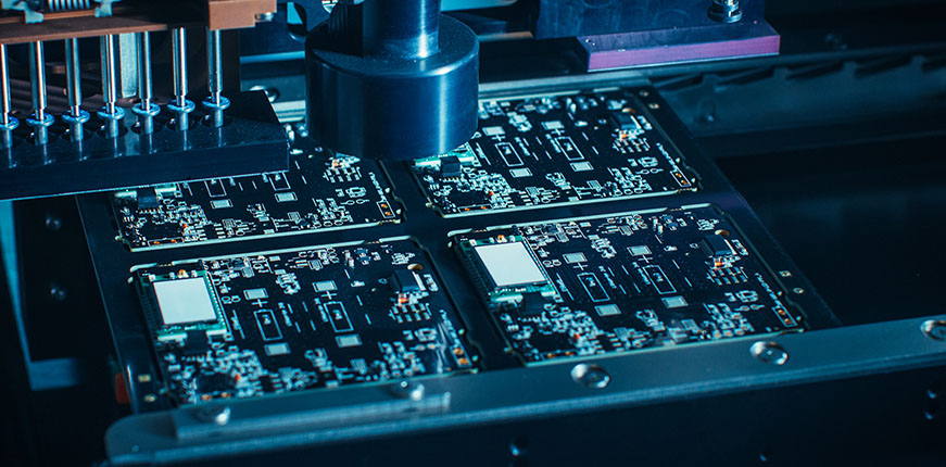
PCB manufacturing is also considered the construction of board design. PCB manufacturing is a two-step process which starts with the board fabrication and ends with the assembly of the printed circuit board.
PCB testing
PCB testing sometime may be referred to as the third stage of development of PCB. This step is generally performed after the manufacturing process. To evaluate the ability of the board to perform its operational functionality the PCB testing has been done. In this stage, if any errors are found in any area of the design, then it should be modified and improved accordingly so that it would be able to satisfy the program requirement and needs.
PCB assembly
PCB assembly is known as the second stage of PCB manufacturing where the components of the board are mounted to the bare board with a soldering process.
PCB fabrication is adopted as the process which can transform a circuit board design into a physical structure based on its specification provided in the design package. The physical structure can be achieved with the following main actions.
- Imaging the layout on copper laminates.
- To reveal the pads and traces the excess copper is removed from the inner layers.
- Creation of the PCB layer by laminating by pressing and heating the boat material at a very high temperature.
- With the help of vias and paints, the next step is to drill holes for mountain holes.
- The next step is to plate the pinholes
- You need to add another protective coating to the surface
- Logos, markings Silk screen printing on the surface
These are the basics of a PCB fabrication process for a circuit. If you want to get the best PCB fabrication then it is advisable to contact Chinapcbone.
ChinaPCBOne Technology LTD. is the author of this article on PCB fabrication. Find more information, about PCB manufacturing.